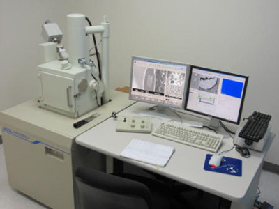
Scanning Electron Microscopy – Tungsten
Microtrace operates two state of the art scanning electron microscopes (SEM): our conventional, tungsten source instrument with thermionic emission (JEOL 6400 LV); and, our high-resolution instrument, a field-emission scanning electron microscope (JEOL 7100FT). SEMs use electrons instead of visible light to create an image, and since an electron has a much shorter wavelength than light in the visible region of the spectrum, much higher magnifications can be obtained (up to 1,000,000 times with the field emission instrument). This allows observations of particles and fine structure as small as 1 nanometer in diameter.
Low Vacuum and Non-Conductive Samples
In most cases, non-conductive samples can be studied using a low vacuum mode, which permits study of samples in a vacuum of 1 to 270 Pa. For more critical imaging, samples can be gold or carbon coated.
Elemental Analysis
Our conventional SEM is equipped with a Thermo Noran SDD EDS detector and has full beam control and stage automation to permit EDS spectral imaging and automated methods such as gunshot residue (GSR) analysis and phase identification analysis.
Related Standardized Methods: ASTM C1723, E1508, E1588, E2809, F1372
How May We Help You?
Contact usto discuss your project in more detail.


